Scanning Electron Microscopy (SEM) is a powerful imaging technique widely used in materials science, biology, and engineering. It uses a focused beam of electrons to scan the surface of a sample, producing detailed images with exceptional depth of field. This technique allows for the examination of microstructures and surface features at magnifications up to several hundred thousand times. SEM is invaluable for analyzing the morphology, composition, and topography of materials.
Typical Applications
- High-resolution SEM imaging
- Electron beam lithography
- Elemental analysis via energy dispersive x-ray spectroscopy (EDS)
Instruments
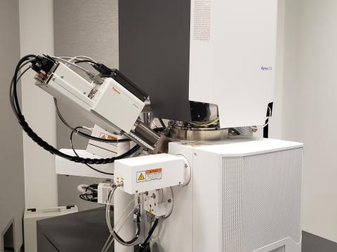
ThermoFisher Scientific Apreo 2 SEM
- High and low vacuum modes for analyzing conductive and insulating samples
- SE, BSE and cathodoluminescence (CL) detectors, insertable CBS detector
- EDS detector
- Nabity NPGS electron beam lithography system
- 5-axes eucentric stage
- Drift-corrected frame integration imaging
- Maps software for large area, high resolution imaging
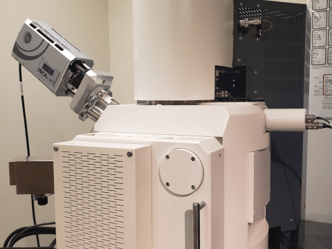
ZEISS Ultra-55 SEM
- Field emission electron beam source with 1nm SEM imaging resolution
- Nabity NPGS electron beam lithography system
- Large chamber capacity
- 5-axes stage able to view/write an entire 4-inch wafer
- In-lens SE, in-lens BSE, and Everhart-Thornley electron detectors
- Oxford 10mm SDD detector for X-ray analysis and mapping
Instrument Contact: camcor@uoregon.edu